
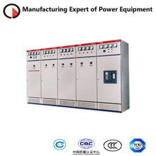
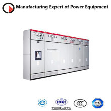
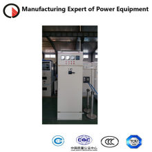
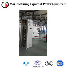
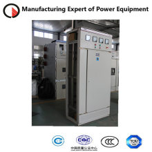
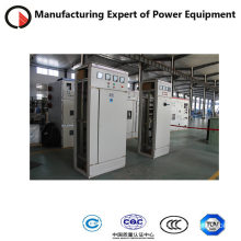
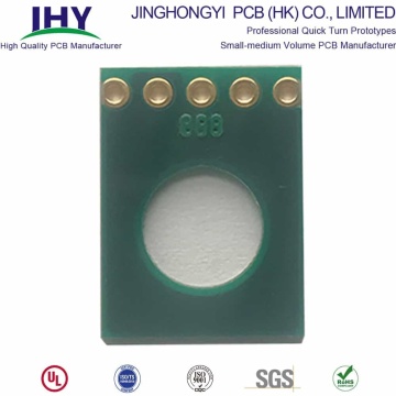
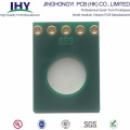
6 Layer 6 OZ Thick Copper PCB for Power Supply
Product Description
6 Layer 6 OZ Thick Copper PCB for Power Supply
Keyword Tags: 6 Layer PCB, Heavy Copper PCB, Thick Copper PCB, Power Supply PCB
Product parameters and technical details
- Layer: 6
- Board thickness: 1.0+/-0.1mm
- Material: Shengyi
- Minimum aperture: 0.4mm
- Surface treatment: Immersion Gold
- Minimum hole copper Thickness: 35um
- Inner Layer Hole Copper Thickness: 160um
- Process characteristics: surface line insulation, thick copper, inductance control
- Application: high-power switching power supply, communication power supply, power inductor, UPS power supply, rail transit power supply, inverter power supply, electric power supply, medical power supply
Thick copper PCB is a layer of copper foil bonded to the printed circuit board's glass epoxy substrate. When the copper thickness is ≥2oz, it is defined as a thick copper PCB or Heavy Copper PCB.
The properties of thick copper PCB: The thick copper PCB has the best elongation, is not limited by the processing temperature, the high melting point can be used oxygen blowing, low temperature is not brittle, and other hot-melt welding methods, and also fire, belongs to non-combustible materials. Thick copper PCBs form a robust and non-toxic passivation coating even in extremely corrosive environments.
Advantages of thick copper PCB: Thick copper PCB is widely used in various home appliances, high-tech products, military, medical, and other electronic equipment. The thick copper PCB application makes the circuit board, the core component of electronic equipment products, have a longer service life. At the same time, it is of great help to simplify the volume of electronic equipment.
In PCB prototype manufacturing, a thick copper plate is a unique process, with specific technical threshold and operation difficulty, the cost is also relatively expensive. Some PCB prototype manufacturers do not want to do it or rarely do it. JHYPCB is a global PCB prototyping services, small and medium volume PCB manufacturing enterprise, dedicated to solving PCB prototyping enterprises for the rugged plate, precision PCB. The special PCB is processing pain points, providing customers with unique laminated thick copper, multi-layer structure, plating nickel/gold finger, special-shaped hole, charged with deep grooves, such as unusual process PCB prototypes, the delivery speed is faster than ordinary factory must be at least a third of the time. At present, in the prototype manufacturing of PCB for this process, JHYPCB can achieve 2~6 layers (more than 6 layers, which need to be reviewed). Maximum copper thickness 10oz; Minimum through-hole 0.4~0.6mm. Welcome the general customers' inquiry.
Why us?
1. High-quality raw materials to create high-stability high-end power thick copper PCB
- Use medium and high TG thick copper-clad laminates from high-end brands such as Shengyi and Lianmao to ensure that the copper thickness meets the design requirements.
- Imported drill bit and electroplating solutions are used to ensure the flatness and copper thickness of the hole and increase the high-end power supply's service life.
2. Rich experience in process control of power supply products, providing thick copper power PCBs for many large high-end power supply manufacturers
- Dozens of technical teams engaged in thick copper power PCB processing have rich experience in various control points of thick copper power circuit boards.
3. Superb high-end power supply thick copper circuit board processing capabilities to meet the PCB customization requirements of various high-end power supply manufacturers.
- The number of processing layers can be up to 18, and the maximum copper thickness to be processed is 6OZ for multiple layers and 12OZ on both sides.
- The minimum processing aperture can reach 0.3mm, the maximum plate thickness can be processed to 6 mm, and the insulation layer withstand voltage is above 2000V
4. Advanced processing equipment and sophisticated testing equipment provide a guarantee for the performance consistency of power products
- Advanced Hitachi drilling rigs, sandblasting mills, laser exposure machines, and other process equipment and testing equipment ensure the processing accuracy of lines and holes.
- The introduction of advanced long-arm thickness gauges, two-dimensional gauges, and other testing equipment to ensure that the overall dimensions of each PCB produced are tightly matched
5. Strict quality control system to ensure various functional indicators of thick copper power PCB
- All products are subject to strict performance index tests, such as high and low-temperature cycle aging test, hole copper test, impedance test, thermal stress test, peel resistance test, solderability test, open and short circuit test, etc.
- Obtained several international quality certifications such as ISO9001 and carried out various quality activities in strict accordance with international quality standards.
As The Best Multilayer Heavy Copper PCB + PCBA Manufacturer in China, We Are Your Best Choice.
Custom Quote Requipment
To ensure an accurate quote, be sure to include the following information for your project:
- Complete GERBER files including the BOM list
- Other file types (Altium, Protel, Or CAD)
- "Read Me" notes for additional fabrication information
- Quantities
- Turn time
- Panelization Requirements
- Materials Requirements
- Finish requirements
Inquiry Notes
As is known, PCB and PCBA is a customized product, so the details, please contact us and a quotation will be offered.
Please send us PCB files in gerber files, ".pcbdoc", ".lay", ".lay6" or ".brd", "CAM350 RS274X", "Protel 99SE", "P-CAD 2001 PCB", etc. For the PCBA quotation, the BOM list in the format of "xls" is also needed.
Your custom quote will be delivered in just 2-24 hours, depending on the design complexity.
We can support your research and development efforts and meet your fast life cycles. We have set a separate department where the exclusive production planner will follow your orders' production to meet the requirements of Rapid PCB Prototyping and Quick Turn PCB.
1) We do PCB from double side up to 30-layer Multilayer PCB, HDI jobs.
2) If you have repeat orders from other suppliers and transfer to JHYPCB, we can accept FREE OF TOOLING.
3) Except for excellent quality and professional service, we also pay every detail for our customers, for example, package to use Desiccant packs & moisture indicator in the vacuum-sealed pack to protect PCB.
4) Material: We have FR4 TG135/TG158/TG180 normal material in stock, also have FR1/ FR2/ FR3/ CEM1/ CEM3/ ROGERS/ ARLON/ ISOLA.
5) Rigid / flex/ flex-rigid PCBs with UL approved.
6) Flexible, quick feedback for customers always.
7) Quickly offer will be less than 2 hours. Some top urgent inquiries we can offer within 1hour.
We provide one-stop PCB/PCBA customization services. To meet all of customer's PCB/PCBA requirement is JingHongYi PCB service's goal.
1. To offer good quality PCB/PCBA to our customer, we will do many kind of testing to ensure quality before shipment
2. Outgoing test to check min PTH Cu thickness, Min surface Cu thickness, ENIG Au data,Ni data, Au layer adhesion testing, soldermask adhesion testing, silkscreen adhesion testing, Thermal stress testing, hardness testing, Twist testing, Bow testing
3. Microsection testing to check hole Cu thickness, Surface Copper thickness, Wrap copper thickness, Hole Wall Integrity, soldermask thickness and stack up.
4. E-test to check any open/short circuit.
5. Thermal Stress Test to avoid any Delamination, Measling and others.
6. Solderability of PTH to avoid any discolor, Wrinkles, Blisters, Measling, Blow-Hole, Solermask peel off, and soldermask filled in hole-wall incompletely.
Impedance testing, and so on...

JingHongYi PCB (HK) Co., Limited - Quick Turn PCB Prototype and Tricky PCB Expert.
Professional and Quick Turn High-quality PCB Manufacturer in China.Offers One-stop PCB Manufacturing and PCB Assembly Services, Including PCB Fabrication, Electronic Components Procurement, Stencil, and Assembly.
Jinghongyi PCB (HK) Co., Limited is a professional manufacturer of high-quality PCB. JHY PCB specializes in Quick Turn PCB prototypes, small-medium volume PCB. Established in 2011, located in Baoan District, Shenzhen, China, with more than 500 experienced employees, we're able to achieve a monthly output of 40000 square meters.

PCB Manufacturing Services
As one of the leading Printed Circuit Board manufacturers based in China, JHYPCB has been offering international companies of all sizes with high-quality PCB prototype to production services at a fair price for 8 years. To make professional and advanced circuit boards, we're committed to adhering to the strictest standards during the PCB manufacturing process, we're fully compliant with the ISO 9001:2008 quality management system.
- A professional and trustworthy PCB Prototype manufacturer.
- Fastest PCB Prototype.
- One-stop solution for various PCB& SMT Stencil.
- Low cost for simple PCB.
- Affordable price for high-tech PCB.
- Minimum orders 1pcs.
- 24-hour online customer service.
- Professional PCB engineer for one-to-one service.
- Shipment on time.
- Guarantee good service and quality from PCB quotation to delivery.
PCB Assembly Services
To deliver true value and convenience to our PCB fabrication clients, we expand our business to components sourcing and turnkey PCB assembly services ranging from the prototype, low-to-middle volume to high volume up to 1 million pcs. We can mount components on circuit boards using surface mount technology (SMT), through-hole technology (THT), and manual insertion:
- No minimum order
- No additional charge for stencils
- Free DFM Check
- 100% AOI test and X-Ray test for BGAs package
- Function tests & IC programming based on custom requirements
All boards are produced according to IPC-6012 standards and inspected according to IPC-A-600 in the latest version. Our products are widely applied in communications, industrial control, power electronics, medical equipment, security electronics, consumer electronics, LED, etc. More than 90 percent of them were exported to Europe, North America, South America.
One-stop Service Include
| PCB Prototype | Quick Turn PCB | Single-Sided PCB |
| Double-Sided PCB | Multilayer PCB | Rigid PCB |
| Flexible PCB | Rigid-Flex PCB | LED PCB |
| Aluminum PCB | Metal Core PCB | Thick Copper PCB |
| HDI PCB | BGA PCB | High TG PCB |
| PCB Stencil | Impedance Control PCB | PCB Assembly |
| High-Frequency PCB | Bluetooth Circuit Board | Automotive PCB |
| USB Circuit Board | Halogen-Free PCB | Antenna PCB |
PCB Factory and Workshop
Advanced Production Equipment, Skilled Technical Workers are the Guarantee of Product Quality.
We Guarantee to Provide Reliable Products Based on Advanced Manufacturing Testing Equipments, Well-known Raw Materials and Comprehensive Management Systems.


PCB Assembly (PCBA) Equipment

Applications
JHYPCB's Products are widely used in communication equipment, industrial control, automotive, medical equipment, security electronics, consumer electronics, aerospace and other high-tech fields. Over 80% of its products are sold in more than 40 countries and regions, including the United States, Europe and Asia (excluding China).

PCB Fabrication and Assembly Capability
At JHY PCB We Have One of The Best State-of-the-art Production Facility for PCB and PCB Prototype Fabrication in the World Which is Handled by the Best Professionals You Can Find Anywhere.PCB Fabrication Handled By Professionals
We encourage electronic, computer and other related manufacturers to let our professionals handle all their PCB fabrication and PCB Prototype fabrication needs.- At JHY PCB we have one of the best state-of-the-art production facility for PCB and PCB Prototype Fabrication in the world which is handled by the best professionals you can find anywhere.
- Our professionals bring in a lot of expertise, passion and technology into the design and assembly methods for circuit boards with high accuracy, speed and ease.
- We encourage electronic, computer and other related manufacturers to let our professionals handle all their PCB fabrication and PCB Prototype fabrication needs.
What Our Clients Get from our PCB Prototype Fabrication
- Professional technology service
- Feasibility manufacturing suggestion
- Expedited Delivery
- Online Quote
- Low Prices
- One-stop purchase Solution
Lead Time - Quick Turn and Fast Delivery

| |||
| Item | Manufacturing Capability | ||
| PCB Layers | 1~30 Layer | ||
| Quality Grade | IPC Class 2, IPC Class 3 | ||
| Laminate | FR-4, S1141, S1000-2, IT180A, Isola-FR408HR, FR406, Isola 370 HR, Rogers, Taconic, Arlon, Halogen Free, etc. | ||
| Brand of Laminate | Kingboard, ITEQ, Shengyi, Nanya, Isola, Rogers, etc. | ||
| Max Board Size | 533.4 * 762 mm | ||
| Board Thickness | 0.1~8.0mm | ||
| Board Thickness Tolerance | ±0.1mm / ±10% | ||
| Copper Thickness | Outer layer:1/3oz~10oz, Inner layer:1/2oz~6oz | ||
| Min Mechanical Drilling Hole Size | 6mil(0.15mm) | ||
| Min Laser Drilling Hole Size | 3mil(0.075mm) | ||
| Min Line Width/Line Space | 2/2mil(Outer layer:1/3oz,Inner layer:1/2oz) | ||
| Surface Finishes | OSP, HASL, HASL Lead-Free (HASL LF), Immersion Silver, Immersion Tin, Plated Gold, Immersion Gold(ENIG), ENEPIG, Golden Finger+HASL, ENIG+OSP, ENIG+Golden Finger, OSP+Golden Finger, etc. | ||
| Solder Mask Colors | Green, Red, White, Black, Blue,Yellow, Orange, Purple, Gray, Transparent .etc. | ||
| Matte: Green, Blue, Black, etc. | |||
| Silkscreen Colors | Black, White, Yellow, etc. | ||
| Electrical Testing | Fixture / Flying Probe | ||
| Other Testing | AOI, X-Ray(AU&NI), Two-dimension Measurement, Hole Copper Instrument, Controlled Impedance Test(Coupon test&Third Party Report), Metalloscope, Peeling Strength Tester, Solderability Test, Logic Contamination Test | ||
| Special Capabilities | Thick Copper, Thick Gold(5U"), Gold Finger, Blind and Buried Hole, Countersink Hole, Semi-hole, Peelable Mask, Carbon Ink, Counter sink hole, Plated board edge, Press fit hole, Control depth hole, VIA in PAD, Non-conductive resin plug hole, Plating plug hole, Coil PCB, Super Mini PCB, Peelable Mask, Carbon Ink, Controlled Impedance PCB, etc. | ||
Why Choose us
As a High-end Circuit Board Manufacturer, JHYPCB Has the Ability to Provide a Variety of Tricky PCBs Manufacturing. Fast Delivery, Quality Assurance is Our Core, One-stop PCB Circuit Board Manufacturing and PCBA Assembly Services, To Save Time and Cost for Customers. 
Certificate
UL, TS16949, ISO-9001, and RoHS Compliance.
Quality Assurance
Incoming Quality Control
In-Process Quality Control
Final Quality Control
One-step Service From PCB Manufacturing to PCB Assembly

Visit Factory and Exhibition

Excellent Suppliers - SM ink, CCL, Chemical

8 Advantages
1. Diversified Production Capability
5G Mobile Communication. Taconic/Rogers/Arlon PCB. Heat sink PCB/AL PCB. Antenna PCB. PA PCB/Hybrid PCB. High Precision Multilayer / Impedance PCB. Half hole PCB/film cover PCB. Other special PCB. Normal FR-4 PCB.
2. High Cost Performance Ratio
Own PCB manufacturing and PCB assembly factory,We can provide the most cost-effective products.
3. Stable and Fast Delivery Performance
1L:12 hours
2L:12 hours
4L:12 hours
6L:12 hours
4. Personalized Service
Technical support engineers provide one-to-one service from product proofing to mass production to after-sales, realizing order online tracking and after-sales service.
5. Rapid Order Response
Quotation System: Quote within 24 Hours
Service System: Respond within 30 Minutes
EQ System: Nearly 30 technical support teams responded quickly within 24 hours
Language services: Chinese, English, Korean, Japanese and Vietnamese
6. Stable Quality
Excellent QA, production management system and technology team to assure quality.
7. Advanced Technology and Equipment
JHYPCB has a strong technical team and advanced PCB manufacturing equipment, which can provide excellent technical support and after-sales service in an all-round to provide customers with efficient manufacturing and reliable products.
8. Advanced Management System SQM
SQM regularly audits qualified raw material suppliers to promote continuous improvement and ensure quality.
CRM regularly collects customer needs and problems to better provide customers with quality solutions.
ERP can track the order status at any time through the production base ERP system.
Package and Shipping

JingHongYi PCB (HK)CO., Limited
As a high-end circuit board maanufacturer, JHYPCB has the ability to provide a variety of tricky PCBs manufacturing.
- Specialized in high density, high difficult technology
- 99%+ customer satisfaction rate
- Diversify PCBs manufacturing
- Competitive price & NO min order quantity required
- No additional tooling charge for PCB reorders
- Quality guaranteed services
- Quick-turn around delivery time, 24 hours delivery available
- Free DFM check by professional engineers
- Knowledgeable support team available via phone and email
- Function test based on customer's specific requirements

Q1: What service do you have?
A: We are the factory, we have our PCB manufacturing & Assembly factory.
We can offer a one-stop service from PCB manufacturing to PCB assembling, testing, housing, and other value-added services.
Q2. What is needed for PCB or PCBA quotation?
A: PCB: Quantity, Gerber file and Technic requirements(material, surface finish treatment, copper thickness, board thickness,...)
PCBA: PCB information, BOM,Testing documents...)
Q3. What file formats do you accept for PCB and PCBA production?
A: Gerber file: CAM350 RS274X
PCB file: Protel 99SE, P-CAD 2001 PCB
BOM: Excel (PDF,word,txt)
Q4: What any other information should be offered except for the file?
A5: Following specifications are needed for the quotation:
a) Base material
b) Board thickness:
c) Copper thickness
d) Surface treatment:
e) color of solder mask and silkscreen
f) Quantity
Q5: What is your minimum order quantity?
A: Our MOQ is 1 PCS.
Q6. Shipping cost?
A: The shipping cost is determined by the destination, weight, packing size of the goods. Please let us know if you need us to quote you the shipping cost.
Q7: Are my PCB files safe when I submit them to you for manufacturing?
A: We respect customer's copyright and will never manufacture PCB for someone else with your files unless we receive written. Permission from you, nor we'll share these files with any other 3rd parties.
Q8: No PCB file/Gbr file, only have the PCB sample, can you produce it for me?
A: Yes, we could help you to clone the PCB. Just send the sample PCB to us, we could clone the PCB design and work out it.
Q9: What payment do you accept?
A:-Wire Transfer(T/T)
-Western Union
-Letter of Credit(L/C)
-Paypal
-Ali Pay
-Credit Card
We recommend bank transfer.
Q10: How to get the PCBs?
A: For small packages, we will ship the boards to you by DHL, UPS, FedEx, EMS. Door to door service! You will get your PCBs at your home.
For bulky goods more than 300kg, we may ship your PC boards by ship or by air to save freight costs. Of course, if you have your forwarder, we may contact them for dealing with your shipment.
Q11. How about the delivery?
Usually, for sample order, our delivery is about five days. For small-batch, our delivery is about seven days.
For the mass production batch, our delivery is about ten days.
But that depends on the real condition when we get your order.
If your order is urgent, please contact us directly, we will make a priority to deal with it and do our best to give you a satisfied delivery time.
Q12: How about your factory production capacity?
A: we can provide 40000 square meter/month.
Q13: Which countries have you worked with?
A: US, Canada, Italy, Germany, Czech Republic, Australia, Japan, Spain, Portugal, France, Britain, Poland, Ukraine, Russia, Brazil, Argentina, and so on.
Q14: How do you ensure the final quality of the product
For PCB, we will use the Flying Probe Test, E-test, etc. for it.
For PCBA, we need you to offer us a method or test fixture for the function test. Before that, our inspectors will use a microscope and X-ray to check the IC foot welding or bad solder, etc.
Q15: Will you check my files before production?
A: Yes, our engineer will check your Gerber file and BOM list to avoid any mistake.
Q16: My budget is limited; can you provide solutions to save cost?
A: Yes, we can. For example, for PCBA: Replace the DIP components with SMD components, so it can narrow the PCB board size to save cost. Re-layout the PCB to reduce the size, it can save cost. Also, we can recommend alternative components.
Q17: Do you accept process materials supplied by clients?
A: Yes, we can provide the component source, and we also accept component from the client.
Q18: Can we visit your company?
No problem. You are welcome to visit us in Shenzhen.
Contact us if you need more details on 6 OZ Copper Thickness. We are ready to answer your questions on packaging, logistics, certification or any other aspects about Thick Copper Power Supply PCB、Heavy Copper Power Supply PCB. If these products fail to match your need, please contact us and we would like to provide relevant information.
Product Categories : Thick Copper PCB